
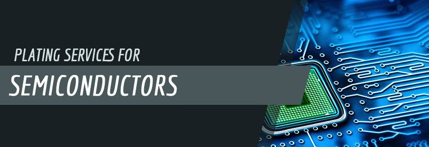
Plating Services For Semiconductors
Semiconductors are the foundation of the electronics industry. These partially conductive products include transistors, chips and other electronic control parts, and are integral to electronic equipment from mobile phones to cars and robots.
Today, companies create most semiconductor chips using silicon plated with another material. This outer coating protects the semiconductor from outside elements and connects it to the outside world. These plating materials can be anything from tin to gold, and each has a unique set of traits with different effects on the finished product.
To help better understand the role of plating in the manufacturing of semiconductors, here is a guide to semiconductor plating.
Semiconductor Basics
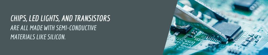
Chips, LED lights, and transistors are all made with semi-conductive materials like silicon. This means the material has characteristics of both conductors and insulators, but doesn't fit into either category. In order to produce these parts, the material must undergo several manufacturing processes:
- Wafer Production: Semiconductors usually start as a wafer-thin slice of a purified semiconductor material. Usually these wafers are produced by heating the material, molding it, and processing it to cut and grind it into small, smooth wafers.
- Deposition: The prepared wafers are cleaned, heated and exposed to pure oxygen within a diffusion furnace. This results in a reaction that produces a uniform film of silicon dioxide on the surface of the wafer.
- Masking: Also called photolithography or photo-masking, this process protects one area of the wafer while another is worked on. After applying a light-sensitive film to one part of the wafer, an intense light is then projected through a mask onto it, exposing the film with the mask pattern.
- Etching: To start the etching process, manufactures bake the wafer to harden the remaining film pattern, and then expose it to a chemical solution to eat away the areas not covered by the hardened film. After this, the film is removed and the wafer inspected to ensure proper image transfer.
- Doping: Atoms with one less or one more electron than the material are introduced into the exposed wafer area to alter the electrical properties of the silicon. For silicon, these are boron and phosphorous respectively. Adding atoms with one more electron is termed as N-type doping, because it adds a free electron to the silicon lattice, giving the material a negative. Adding atoms with one less electron is termed as P-type doping, because they create holes in the silicon lattice where a silicon electron has nothing to which it can bond. This creates a positive charge. Both doping types turn the semiconductor into a excellent conductor. The manufacturer the repeats these steps, deposition through doping, are repeated several times until the last layer is completed and all active circuits are formed.
- Dielectric Deposition and Plating: Following the conclusion of the internal parts of the semiconductor, the manufacture connects the devices by adding layers of metals and insulators. This both protects these circuits and creates a connection between the inner workings of the semiconductor and the outside world. A final insulating layer is added to protect the circuit from damage and contamination. Openings are etched into the film to allow access to the top metal plate.
As discussed, plating is one of the last steps in the semiconductor manufacturing process, but holds an important role as protective shell and interactive layer between the semiconductor's internal circuits and the outside world.
The Plating Process
Manufacturers often plate semiconductors using a process called electroplating. Also known as electrodeposition, this process deposits a thin layer of metal on the surface of a work piece referred to as the substrate. The basic process is as follows:
- The plating metal is connected to the positively charged electrode of an electrical circuit. This electrode is called the anode.
- The work piece, or substrate, is placed at the negatively charged electrode, called the cathode.
- Both the plating metal and the substrate are immersed in an electrolytic solution called a bath.
- After submersion, a DC current is supplied to the anode, oxidizing the atoms of the plating metal and dissolving them into the bath. At the cathode, the negative charge reduces the atoms, causing them to plate the substrate.
This general process describes most electroplating. However, semiconductor electroplating is much smaller in scale than the average electroplating processes. The chips in question are often less than an inch in diameter, and the circuits inside them consist of miniscule wires. Any errors, such as breakage or the addition of dust particles to the semiconductor, can result in a defective product. As a result, semiconductor electroplating involves a few extra precautions and considerations in order to ensure the quality of the finished product.

Semiconductor electroplating differs somewhat from regular plating in the following ways:
- Clean Environments: The fine detail in semiconductor plating requires an extremely clean environment. For this reason, plating work for semiconductors takes place within a clean room with less than one ten-thousandth, or 0.01%, of the amount of dust found in outside air.
- Filtered Plating Solutions: The requirement for a clean environment further applies to the plating solution, also called a bath. This bath is filtered closely to remove dust and other particles, preventing defects and impurities.
The result of this process is a thin exterior coat of metal for the semiconductor. This layer can be stacked atop or between other layers until the desired thickness is reached.
The Benefits of Plating for Semiconductors
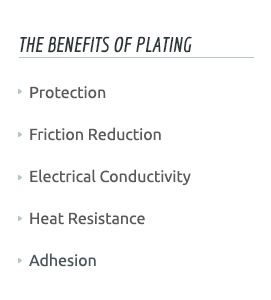
Semiconductor plating serves a number of functions, which directly affect the performance of the semiconductor as a whole. Different materials produce unique sets of features and benefits to the semiconductor, including the following:
- Protection: Some materials create a barrier on the substrate, protecting it from atmospheric conditions to prevent corrosion. This increases the life of the semiconductor and guards it from extreme conditions.
- Friction Reduction: Some materials reduce the build-up of friction in products like electrical connectors. This improves performance and reduces premature wear and tear.
- Electrical Conductivity: Some plating enhances electrical conductivity, making the product more electrically efficient.
- Heat Resistance: A few plating materials are able to withstand extremely high temperatures, protecting the semiconductor from damage caused by extreme heat. This can increase the semiconductors' lifespan substantially.
- Adhesion: A few materials provide an excellent undercoating to promote adhesion to another coating. This increases both the quality and the longevity of the plating as a whole.
The electroplating process itself multiplies these benefits, which improves corrosion resistance, enhances electrical conductivity, increases the solderability of the substrate and protects it against wear.
Plating Materials Optimal for Semiconductors & Electronic Components
Each plating material has a specific set of properties that affect the performance of the semiconductor it plates. In order to help choose which metal is the best plating material for your semiconductors, here is a summary of each plating material and what it does for the semiconductor:
Tin and Tin Alloys
The electroplating of tin, also called "tinning", is a cost-effective alternative to plating with gold, silver or palladium. Unlike these materials, tin is abundant and cheap, although it's not as conductive as other materials. Additionally, tin has the disadvantage of forming sharp protrusions, called whiskers, which can damage any materials surrounding it. SPC has developed a way of avoiding this by using a tin-lead alloy. This alloy naturally reduces the occurrence of these protrusions, and does not require an undercoating, unlike tin. Tin and its various alloys are used in semiconductors for corrosion protection.
Recent concerns over the impact of heavy metals on the environment have led researchers to search for replacements to the lead soldering used to connect electrical components. In an effort to become lead-free, many companies are turning to pure tin, which has good adhesiveness, to solder. Tin can also eliminate the need for lead soldering when used as a plating material.
Copper
Most people are aware of copper's exceptional conductive properties, which is why copper plating for semiconductors is quite common. This soft metal is extremely valuable in electronics manufacturing, offering both electrical and thermal conductivity. While it's possible to use it by itself, copper often receives an additional metal coating to prevent corrosion and enhance the electrical properties of the other materials.
Nickel
Nickel plating is valued for its evenness and chemical resistance. This material is often used to protect against corrosion, or as a base layer for gold or silver. Nickel often appears as an alloy, combined with zinc or palladium to take on some characteristics of these metals.
Silver
Another precious metal, silver is also used for plating. While less expensive than gold or platinum, silver still offers several important benefits, including thermal and electrical conductivity, corrosion resistance and compatibility with several other types of metals. Manufactures often use silver to provide a coating on more active copper parts, because of its low contact resistance and strong soldering characteristics.
The primary drawbacks for silver include its relatively high cost and its tendency to tarnish. This tarnishing tends to reduce the shelf life of most silver-plated products.
Gold
Gold plating for semiconductors is very expensive, but highly valued. This coveted metal is highly conductive and heat resistant, and serves as an excellent barrier to corrosion. Most commonly, gold plating is applied on top of nickel, which acts as a corrosion inhibitor by preventing rust from penetrating pores in the surface of the gold layer. It also prevents the diffusion of other metals into the gold surface, causing it to tarnish. This tends to happen with zinc and copper.
The cost of the material is its only downside, and as a result, gold layers tend to be as thin as possible for the application.
Request a free quote
For Plating for Semiconductors
Palladium and Palladium Alloys

Palladium is a relatively soft metal, making it a poor plating material in its pure form. However, palladium-cobalt alloys are excellent plating materials, as manufactures can easily control the thickness of the material. Palladium-cobalt also offers protection against corrosion and wear. Palladium-nickel is another popular alloy of palladium commonly used in applications requiring low surface contact resistance.
Recent hikes in gold prices have led professionals to consider palladium and palladium-alloy plating as a cheaper alternative, saving up to 90% of plating costs. Additionally, palladium is less dense than gold, resulting in lighter finished products with the same coating thickness. Though previously scorned for its lesser performance compared to gold, palladium and its alloys are now a leading alternative in efforts to replace and reduce gold in the plating industry. It's now often found in electronic and semiconductor manufacturing.
Platinum
Platinum is an extremely rare and expensive material, even more expensive than gold. However, platinum is an exceptionally smooth-surfaced and durable material that protects against corrosion. Manufactures primarily used it as a protective coating on low-voltage, low-energy contacts.
Platinum plating has recently attracted attention for its applications to fuel cells. Fuel cells are a new, more eco-friendly system of electricity generation. These fuel cells work by combining hydrogen and oxygen to create water — this reaction generates electrical energy. Platinum electrodes are used at the center of this system, but are currently being modified to reduce the costs of fuel cells before they begin mass production.
How to Choose the Right Plating Material
With so many options to choose from, it can be difficult to choose the metals with which to plate your semiconductors. Some are more viable options than others for the type of semiconductor you are producing. Some basic considerations for the type of metal to use include:
- Appearance: Sometimes, the appearance of the semiconductor may be a factor in the final decision, in which case a gold or silver plating should be used.
- Damage Prevention: Some metals, like tin, run the risk of producing protrusions that can damage the finished product. Choose other metals to coat the semiconductor with if this is a concern.
- Specifications: Ensure whichever metal you choose fits the specifications if its particular application.
- Lifespan: Choose a coating that will last as long as the product itself, and help preserve the product as much as possible.
- Environment: Some heavy metals, like lead, have a negative impact on the environment when discarded. For this reason, you should give some thought to eco-friendly plating.
- Other Metals: If using copper as a base coat, it would be unwise to plate gold directly on top of the base layer. Using an intermediary like nickel is necessary to preserve the luster of the exterior gold plating. Watch out for these sorts of interactions to help decide which metals to plate with.
Above all other metal plating considerations, it's important to consult an expert with experience in the craft. An expert can discuss potential problems and considerations that can affect your final plating decisions.
Sharretts Plating Company consists of experts with more than 90 years of metal finishing experience. We can help you select the best process for your equipment and provide advice as to the types of metals you should consider for plating. Contact Sharretts Plating Company for a free quote and more information about the plating services we provide!
LEARN WHAT OUR MANY SATISFIED CUSTOMERS HAVE TO SAY ABOUT Us
"I would like to thank you for the help you have provided us in developing an electroless nickel plating technique on an unusual substrate. The sample platings you provided show that we should be able to reach our goals. I especially appreciate your willingness to take on an unusual job, with the uncertainties that that entails...We are looking forward to working with you in the future on our plating needs."
– Robert K.
