What Is the Difference Between OSP and ENIG? A Complete PCB Finish Comparison
March 18, 2026 | webfx | Share
The surface finish selected for printed circuit board (PCB) fabrication is a critical determinant of manufacturing yield, solder joint reliability, shelf life and ultimate field performance.1
Among the options available, two finishes dominate — organic solderability preservatives (OSP) and electroless nickel immersion gold (ENIG).2 Each technology takes different approaches to protecting copper circuitry and ensuring robust interconnects.
This guide explores the technical differences between OSP and ENIG to provide a framework for selection based on performance metrics, application requirements and total cost of ownership. By examining the underlying chemistry, failure mechanisms and industry standards associated with each, engineers and procurement managers can make decisions that align with their specific reliability goals.
Author’s note: SPC specializes exclusively in high-reliability metallic finishes. Our expertise lies in processes like ENIG, which are engineered for mission-critical applications where long-term durability and performance are nonnegotiable. SPC does not offer OSP services.
Manufacturing Process Comparison: OSP vs. ENIG
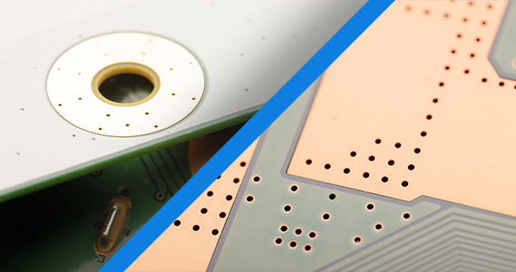
The difference between OSP and ENIG begins at the molecular level. Each finish is rooted in different chemical processes that deposit — or, in the case of OSP, adsorb — the protective layer onto the copper substrate.
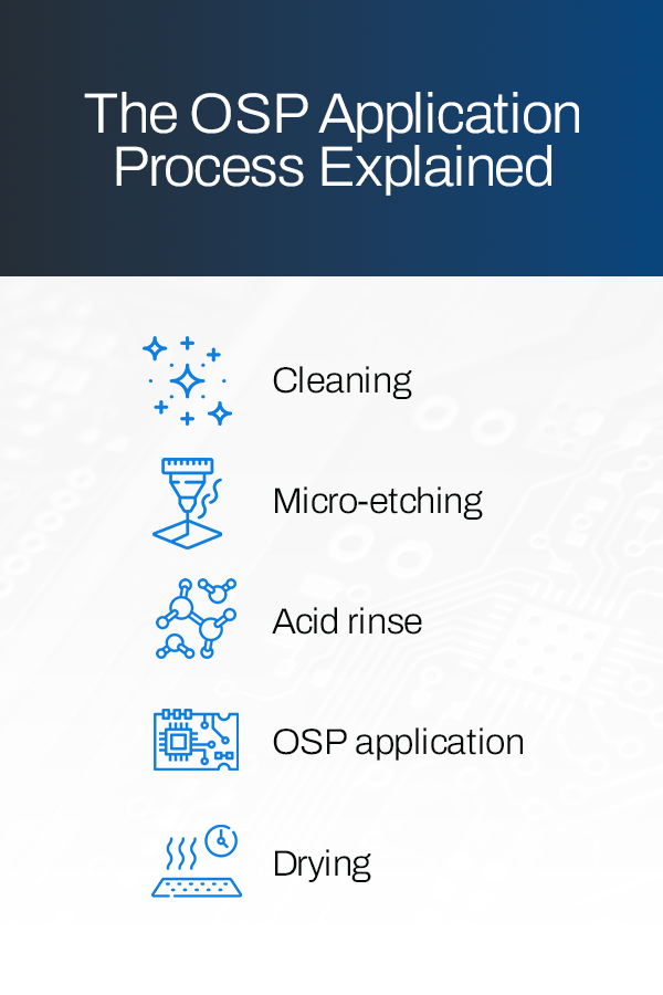
The OSP Application Process Explained
OSP uses a water-based organic compound, typically from the azole family such as benzotriazoles or imidazoles, which selectively bonds to copper.3 The process uses chemical adsorption rather than plating to form an organic layer on the exposed copper areas.
The manufacturing workflow for OSP uses a conveyorized system, characterized by high throughput and relative simplicity.
- Cleaning: The PCB undergoes alkaline or acidic cleaning to remove fingerprints, oils and particulate contamination.
- Micro-etching: A sulfuric acid or peroxide-based etchant is applied to slightly roughen the copper topography. This increases the surface area and enhances the mechanical keying for the organic coating.
- Acid rinse: A sulfuric acid rinse neutralizes any alkaline residues and prevents the drag-in of contaminants into the OSP bath.
- OSP application: The active organic solution is applied. The azole molecules coordinate with the copper atoms to form an organometallic layer. This film is extremely thin, typically ranging from 0.2 to 0.5 microns (2,000 to 5,000 angstroms).4
- Drying: The board is dried to remove moisture and cure the film.
Because the reaction is self-limiting — meaning the film stops growing once a certain thickness is achieved — thickness control is inherent to the chemistry, provided the dwell time and temperature are maintained within process windows.
The Step-by-Step ENIG Plating Process
In contrast, the ENIG process is a complex, multistage electroless depositing sequence that creates a bi-metallic structure. It deposits a barrier layer of nickel, followed by a sacrificial layer of gold. This process is far more chemically demanding and requires rigorous bath management.
The ENIG depositing protocol involves these stages:
- Cleaning and micro-etching: Similar to OSP, the copper surface must be pristine and slightly textured to ensure adhesion.
- Activator: A palladium catalyst is deposited onto the copper. Since nickel cannot spontaneously deposit onto copper, the palladium acts as a seed layer to initiate the autocatalytic reaction.
- Electroless nickel deposition: The board is immersed in a nickel-phosphorus bath. A reducing agent, typically sodium hypophosphite, drives the reduction of nickel ions onto the surface. This creates a nickel-phosphorus alloy layer, usually 3 to 6 microns thick, that serves as the diffusion barrier and the solderable surface.
- Immersion gold deposition: The board is immersed in a gold salt solution. Through a galvanic displacement reaction, gold atoms replace surface nickel atoms. This layer is exceptionally thin, 0.05 to 0.1 microns. It protects the nickel from oxidation during storage.
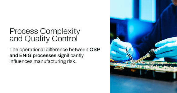
Process Complexity and Quality Control
The operational difference between OSP and ENIG processes significantly influences manufacturing risk.
OSP is a robust, low-maintenance process with fewer chemical variables. Defect modes are generally limited to insufficient thickness or handling damage.
ENIG operates within a tighter process window. The chemical balance of the nickel bath must be meticulously controlled. Deviations can lead to the black pad defect, where the nickel layer is compromised during gold immersion.5 This leads to brittle, unreliable solder joints. To mitigate these risks, reputable plating providers use advanced analytical tools, such as X-ray fluorescence (XRF) for thickness verification and frequent bath analysis.
Technical Performance Comparison: OSP vs. ENIG
When evaluating surface finishes, the main concern for the engineer is how the finish performs under thermal stress, environmental exposure and the soldering process itself.
The following technical comparison explains the strengths and limitations of each.
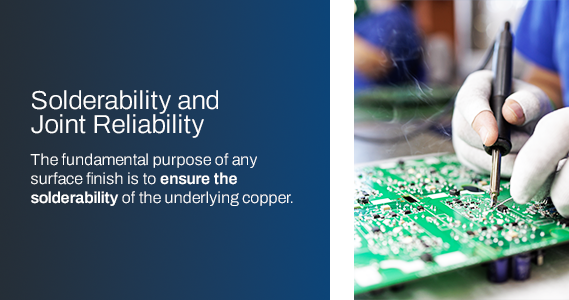
Solderability and Joint Reliability
The fundamental purpose of any surface finish is to ensure the solderability of the underlying copper.
OSP provides a flat surface for accurate solder paste printing. During reflow, the film dissolves in the flux, letting the solder wet the copper directly. This forms a copper-tin intermetallic compound. Although initially strong, the OSP film is fragile. If damaged before soldering, the copper oxidizes immediately, making the pad non-wetting.
ENIG offers superior solderability. During soldering, the gold layer dissolves rapidly into the bulk solder, exposing the fresh nickel layer underneath. The solder then forms a nickel-tin (Ni-Sn) intermetallic bond.6 This Ni-Sn bond is mechanically robust and stable. Additionally, the exceptional planarity of the ENIG finish makes it the premier choice for fine-pitch components, ball grid arrays (BGAs) and flip chips, where even microscopic surface irregularities can lead to coplanarity failures.
Shelf Life and Storage Requirements
The logistical handling of PCBs is often a deciding factor in finish selection, particularly for supply chains with extended inventory hold times.
OSP’s film is highly sensitive to environmental conditions. High humidity and temperature speed up coating degradation. OSP also degrades with handling. Oils and acids from skin can break down the film, causing local oxidation. As a result, OSP-coated boards usually last only 6 to 12 months and need strict storage, such as vacuum packing with desiccant.
In contrast, gold is a noble metal, chemically inert and impervious to oxidation under normal storage conditions. This gives ENIG-coated boards an exceptional shelf life, often exceeding 12 months and, in many cases, remaining solderable for years. It is far more resilient to handling damage and does not require stringent environmental controls.
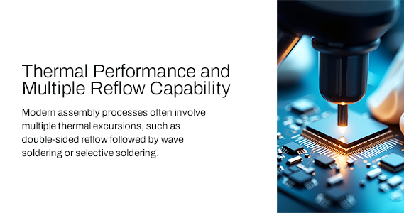
Thermal Performance and Multiple Reflow Capability
Modern assembly processes often involve multiple thermal excursions, such as double-sided reflow followed by wave soldering or selective soldering.
The main weakness of OSP is its thermal instability. The organic film degrades quickly in the presence of heat.7 After the first reflow cycle, the protective coating on the secondary side or through-holes may be compromised, leading to oxidation before the second soldering pass. While high-temperature OSP formulations exist, they still struggle to match the performance of metallic finishes in complex, multistep assembly flows.
The nickel barrier in ENIG is thermally stable. It prevents copper diffusion even at elevated temperatures. This allows ENIG boards to withstand multiple reflow cycles without a degradation in solderability. For complex boards requiring sequential assembly steps, ENIG provides the necessary thermal headroom.
Electrical Performance and Contact Resistance
For applications involving keypads, test points or edge connectors, the electrical surface properties are important.
OSP is nonconductive because it is organic. It cannot be used where direct electrical contact is needed before soldering, such as wire bonding, contact switches or ground points. In contrast, gold offers low contact resistance and high conductivity. This makes ENIG standard for keypads, membrane switches and pogo-pin test points. Its reliable conductivity maintains signal integrity and consistent contact throughout the product’s life.
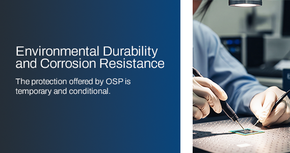
Environmental Durability and Corrosion Resistance
The protection offered by OSP is temporary and conditional. It is designed to survive only until the assembly process is complete. Once the board is fielded, any exposed copper tracks not covered by solder are vulnerable to corrosion.
A key difference between OSP and ENIG is the nickel-gold stack, which provides a formidable barrier against environmental corrosion. The gold protects the nickel, and the nickel protects the copper. This inherent corrosion resistance makes ENIG the preferred option for plating semiconductors and electronics operating in harsh, humid or chemically aggressive environments.8
Application-Specific Considerations
These technical attributes determine which finish suits each industry. Choosing between OSP and ENIG depends on the application’s reliability requirements.
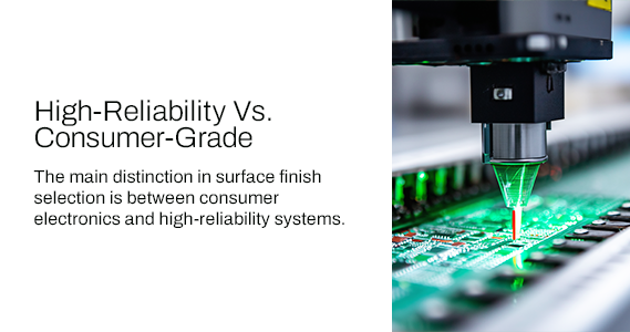
High-Reliability vs. Consumer-Grade
The main distinction in surface finish selection is between consumer electronics and high-reliability systems.
For products like toys, peripherals and disposable Internet of Things (IoT) devices, cost is the main driver. These devices typically have short life cycles of one to three years and operate in home or office environments. OSP is the dominant choice here due to its low cost and sufficient performance for standard assembly.
In aerospace, automotive, medical and industrial control, failure is unacceptable. Boards must withstand thermal cycling, vibration and long service life. ENIG is the standard for these industries. The risk of field failure due to a compromised OSP coating is not an option when human safety or critical infrastructure is at stake.
Fine-Pitch, High-Frequency and Wire Bonding
As electronic designs densify, the physical architecture of the PCB surface becomes a limiting factor. Consideration factors include:
- Fine-pitch components: Devices with pitch requirements below 0.5mm, such as chip scale packages (CSPs) and micro-BGAs, require pads that are perfectly flat. While OSP is flat, its inability to withstand multiple reflows can be problematic for double-sided fine-pitch assemblies. ENIG combines perfect coplanarity with robust solderability, ensuring high yields on high-density interconnect boards.
- Wire bonding: Many advanced semiconductor packages use gold or aluminum wire bonding to connect the die to the lead frame or PCB. OSP is incompatible with wire bonding. ENIG, particularly with specific thickness modifications, or its relative ENEPIG, supports reliable wire bonding, making it indispensable for chip-on-board applications.9
- High-frequency (RF): While ENIG is conductive, the magnetic properties of the nickel layer can impact signal loss in very high-frequency, >10 GHz, applications due to the skin effect. However, compared to OSP, which cannot be used on contact surfaces, ENIG remains the choice for contact points within RF modules. Specialized nonmagnetic electroless nickel options are sometimes explored.
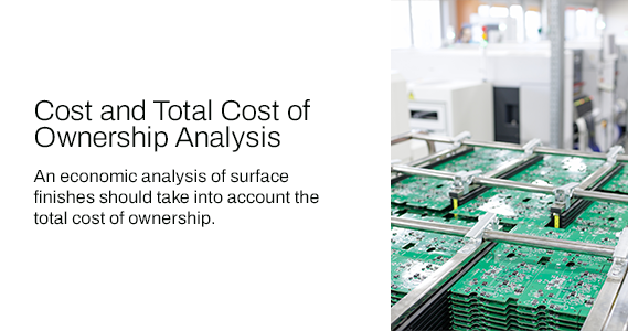
Cost and Total Cost of Ownership Analysis
An economic analysis of surface finishes should take into account the total cost of ownership.
Initial Application Costs Compared
In a direct comparison of invoice price, OSP is the most economical surface finish available.10 The chemistry is inexpensive, containing no precious metals, and the processing equipment has a smaller footprint and lower energy consumption.
ENIG is one of the more expensive finishes. The cost of gold salts is high and fluctuates with the precious metals market. Additionally, the complexity of the ENIG line — requiring more tanks, heaters and analytical equipment — increases the overhead burden.
Rework, Repair and TCO
The cheapest finish on an invoice often becomes the most expensive in practice for high-value PCBs. This paradox is resolved by analyzing the cost of quality:
- Yield loss: If an OSP coating has degraded due to storage or handling, the result is poor wetting during reflow. This requires rework involving manually touching up joints or, in severe cases, scrapping the populated board. The cost of scrapping a board populated with expensive field-programmable gate arrays or microprocessors dwarfs the savings realized by choosing OSP over ENIG.
- Field reliability: A field failure in an automotive braking controller or a medical pacemaker triggers warranty claims, recalls and reputational damage that can cost millions. In these contexts, the premium paid for ENIG acts as an insurance policy. The robust, corrosion-resistant nature of ENIG offsets the risk of latent defects manifesting years after deployment.
While OSP wins on acquisition cost, ENIG often wins on total cost of ownership for complex, high-reliability assemblies.
Industry Standards and Compliance
Adherence to recognized industry standards is essential for ensuring lot-to-lot consistency and reliability. Both finishes are governed by Global Electronics Association (IPC) specifications.11
IPC Standards for OSP and ENIG
Adherence to IPC-4552B is a critical differentiator for plating providers. It signals that the facility has the metrology and process controls necessary to produce a safe, reliable ENIG finish. The following standards apply:
- IPC-4555: This specification covers OSP for printed boards.12 It defines the performance requirements and testing procedures to ensure the OSP coating meets minimum solderability standards.
- IPC-4552B: This is the governing standard for ENIG.13 Revised in 2021, IPC-4552B places strict controls on the thickness of the gold layer, typically 1.96 to 3.94 microinches, and the phosphorus content of the nickel. It also introduced rigorous testing protocols for nickel corrosion. This ensures manufacturers maintain their chemical baths within precise limits.
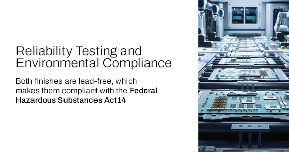
Reliability Testing and Environmental Compliance
Both finishes are lead-free, which makes them compliant with the Federal Hazardous Substances Act14 and United States Environmental Protection Agency Regulations for Electronic Stewardship.15 However, reliability testing, such as surface insulation resistance and electromigration testing, consistently demonstrates that ENIG provides superior insulation resistance in humid environments compared to OSP, which can degrade and absorb moisture.
A Decision Framework for Surface Finish Selection
Selecting the optimal surface finish requires risk and requirement analysis. A three-tiered assessment model can guide this decision.
Tier 1: Absolute Requirements
These are threshold requirements that immediately disqualify a finish if it cannot meet the technical need. Start by answering the following:
- Are there exposed electrical contact surfaces? These might be keypad contacts, edge connectors or test points. If yes, OSP would not be suitable. Its insulating nature prevents reliable electrical contact.
- Does the design require wire bonding? If yes, OSP would not meet your requirements. Only a metallic, bondable surface like ENIG is acceptable.
- Is the board part of a life-sustaining, safety- or mission-critical system? If yes, the inherent risks and limited thermal and environmental robustness of OSP make it a high-risk choice. ENIG is the mandatory starting point.
If your design triggers any of these criteria, the decision is made. If not, proceed to the Tier 2 analysis.
Tier 2: Weighted Performance and Reliability Metrics
This tier involves a semi-quantitative assessment where you weigh the importance of key performance metrics for your specific product. Consider the following factors and assign a rating of “low,” “medium” or “high” importance to each.
Thermal complexity:
- Guiding question: How many thermal reflow/soldering cycles will the board endure?
- OSP assessment: High risk because it degrades after 1 to 2 cycles
- ENIG assessment: Low risk due to its robustness through multiple cycles
Process window:
- Guiding question: How sensitive is my assembly line to process variations?
- OSP assessment: Forgiving with a wider process window
- ENIG assessment: Requires tighter process control
Product service life:
- Guiding question: What is the target operational lifespan of the end product in the field?
- OSP assessment: Poor, as it is suited for short-life products
- ENIG assessment: Excellent, as it is designed for long-term reliability
Environmental exposure:
- Guiding question: Will the product operate in humid, corrosive or uncontrolled environments?
- OSP assessment: Poor, as it offers no long-term corrosion resistance
- ENIG assessment: Excellent, offering an inherent corrosion barrier
Component density:
- Guiding question: Does the design use fine-pitch BGAs, CSPs or high-density interconnects?
- OSP assessment: Adequate — planar, but less robust
- ENIG assessment: Excellent — superior planarity and solderability
If your application rates “high” importance for thermal complexity, service life or environmental exposure, the performance advantages of ENIG justify its selection.
Tier 3: Economic and Logistical Considerations
Once the technical and reliability requirements from Tiers 1 and 2 are satisfied, cost and logistics become the deciding factors.
Supply chain velocity:
- Guiding question: How long will bare boards be stored before assembly?
- OSP assessment: Poor due to short shelf-life, less than 12 months
- ENIG assessment: Excellent due to a long shelf-life, exceeding 12 months
Up-front unit cost:
- Guiding question: Is minimizing the initial per-board cost the main project driver?
- OSP assessment: Excellent with the lowest cost finish
- ENIG assessment: Fair with a higher cost due to the price of gold
Total Cost of Ownership:
- Guiding question: What is the financial impact of a single field failure or manufacturing defect?
- OSP assessment: High risk of yield loss and field failure
- ENIG assessment: Low risk of costly failures
When to Choose Each Finish
The ideal candidate for OSP is a high-volume, cost-sensitive consumer product with a simple assembly process, or single reflow, and a short-to-medium expected service life in a controlled environment. The supply chain must be managed to ensure a just-in-time approach to assembly, minimizing bare board storage time.
ENIG is best for high-value products requiring guaranteed reliability and long-term performance. These complex designs need multiple soldering steps, support fine-pitch components, and must perform reliably in harsh environments. The higher cost is accepted as an investment to avoid more expensive rework or field failures.
Your Partner for Mission-Critical PCB Finishes
In high-reliability electronics, there is no margin for error. While the chemistry of the surface finish is critical, the expertise of the plating partner is equally important. A poorly executed ENIG finish can be as detrimental as a degraded OSP coating.
For over 90 years, SPC has been a leader in industrial metal finishing. For mission-critical applications, standard solutions are not enough. SPC specializes in high-performance finishes, including electroless nickel immersion gold.
Our ENIG lines strictly follow IPC-4552B standards, using XRF analysis and bath control to prevent black pad and ensure consistent gold thickness. For critical applications, our experts ensure your finish meets the highest standards.
Contact us for a quote or to learn how our plating can improve your assemblies’ durability and performance.16

Resources & Insights
Related posts
Explore articles similar to this one
What Is the Difference Between OSP and ENIG? A Complete PCB Finish Comparison
The surface finish selected for printed circuit board (PCB) fabrication is a critical determinant of manufacturing yield, solder joint reliability, shelf life…
Learn more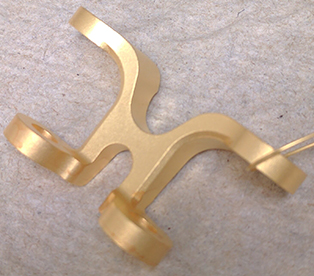
Gold Plating Standards
Gold is known for its glitter and glamour, but it also has significant value from an electroplating perspective. Why should…
Learn more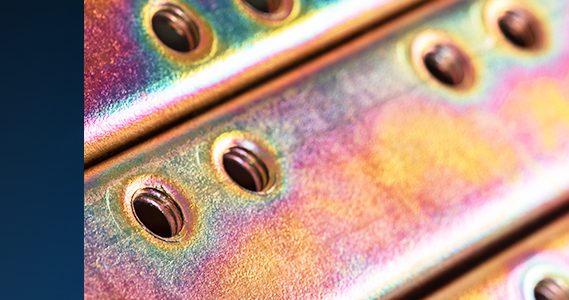
Substrate Effect on Electroplating
How Does Substrate Affect Electroplating? Electroplating depends on the substrate to finish bonds properly and perform effectively. The substrate —…
Learn moreStay in touch
