What Are Semiconductor Nanoparticles?
April 4, 2024 | Stephen Sharretts | Share

Since the creation of nanotechnology, researchers have discovered that specific materials could possess different properties based on their shapes and sizes. This breakthrough has led to the development of various nanoparticles, including carbon-based, ceramic, metal, polymeric, lipid and semiconductor nanoparticles.
Nanoparticles have unique properties that distinguish them from bulk materials, such as a large surface area, surface energy and surface-to-volume ratio. This guide will hone in on a specific nanoparticle group — semiconductor nanoparticles. Here’s your complete breakdown of these particles, including the different types, applications and more.
An Overview of Semiconductors and Nanoparticles
A “semiconductor” is a material that possesses features of both insulators and conductors but doesn’t fall into either category. Semiconductors can be pure elements — like germanium and silicon — or compounds like cadmium selenide and gallium arsenide.1
Many manufacturers use semiconductors for various devices that harness electricity, such as light-emitting diodes (LEDs), chips and transistors. Semiconductors are foundational in manufacturing the electronic devices we rely on daily, including smartphones, televisions, radios, computers and diagnostic imaging equipment.
Nanoparticles are small, crystal-like particles retrieved from bulk semiconductor materials, ranging from 1 to 100 nanometers in size.2 These particles can be agglomerated or loose. They can also have single- or multi-crystal solids or be amorphous. Additionally, nanoparticles take on various shapes, including cylindrical, spherical, hexagonal and conical.
Nanoparticles can be uniform or comprised of several layers. These layers include:
- The surface layer, which contains various small molecules, metal ions or polymers.
- The shell layer, which comprises a chemically different material than the core layer.
- The core layer, or the central part of the nanoparticle.
What Are Semiconductor Nanoparticles and How Do They Work?

Semiconductor nanoparticles — also known as nanocrystals or quantum dots — are tiny, fluorescent particles on the nanometer scale.3 When semiconductor materials are decreased to nanoscale, it significantly alters their chemical and physical properties. Semiconductor nanoparticles feature unique optical properties like spectral diffusion, single-particle blinking and carrier multiplication.
A notable characteristic of semiconductor nanoparticles is the quantum confinement effect, which occurs when a particle’s size is too small to compare with an electron’s wavelength. This results in the nanoparticle’s spatial enclosure of the electronic charge carriers.
Due to the presence of the quantum confinement effect, researchers can leverage the shape and size of semiconductor nanoparticles to accurately tune the energy of electronic optical transitions and energy states. They can adjust the particles’ light emissions throughout the visible, mid-infrared, near-infrared and ultraviolet spectral ranges.
Semiconductor nanoparticles are still in the research phase, but the development and refinement of nanotechnology will surely open doors to major breakthroughs in the semiconductor industry. Researchers are studying and developing these particles to serve a wide range of applications.4 Semiconductor nanoparticles supply a building block for complex nanostructures, like:
- Solar energy conversion
- Cellular and molecular imaging
- Ultrasensitive detection
- Laser technology
- Light-emitting nanodevices
- Nanoscale electronic devices
- Waveguide
- Chemicals
- Biosensors
Examples of Semiconductor Nanoparticles
Semiconductor nanoparticles contain properties of metals and nonmetals. They include compounds of elements in the following periodic table groups:
1. Group II-VI
These semiconductors comprise elements of groups IV and II of the periodic table. They are a special class of materials with properties between those of conductors and insulators. Some examples of II-VI semiconductors include:
- Cadmium sulfide (CdS): CdS is a yellow salt that naturally occurs as two different crystal structures — cubic hawleyite and hexagonal greenockite. CdS has a narrow energy gap, which is why this chemical compound is often used in solar photocatalysis. However, it emits high levels of photocorrosion, causing toxic amounts of Cd2+.5
- Cadmium selenide (CdSe): CdSe is a red-to-black solid that is transparent to infrared light. While it can take on three crystalline structures, the hexagonal wurtzite structure is the most prevalent.
- Cadmium telluride (CdTe): CdTe is a crystalline compound that comprises tellurium and cadmium. It’s typically used as a solar cell material and an infrared optical window.6
- Zinc sulfide (ZnS): ZnS is a naturally occurring salt with two primary crystalline forms — sphalerite and polymorphs — which usually have a cubic crystal structure. A less commonly seen structure is wurtzite, which contains hexagonal crystals. It can be created by heating sphalerite to 1020 degrees Celsius.7
- Zinc selenide (ZnSe): ZnSe is a bright yellow binary solid compound that rarely occurs in nature. The most frequently used substrate is ZnSe cooled to the temperature of liquid nitrogen.8
- Zinc telluride (ZnTe): ZnTe is an intrinsic, moderately toxic semiconductor with a cubic crystalline structure. It has reddish crystals that decompose in water and melt at 1238 degrees Celsius.9
- Zinc oxide (ZnO): While ZnO is present in the Earth’s crust as the mineral zincite, this compound is generally produced synthetically for commercial applications. ZnO occurs as a white powder, which is nearly insoluble in water. It is in a broad range of products, including ceramics, plastics, rubbers, batteries, paints, cement, glass, lubricants, pharmaceuticals, fire retardants, and protective coatings.10
In these types of nanostructures, the shell material’s conduction band — which is a higher bandgap material — has a higher energy than the core.11 Meanwhile, the shell’s valence band has a lower energy level than the core. Holes and electrons are confined in the core.
2. Group III-V
A III-V semiconductor combines gallium and arsenide or gallium and nitride. Gallium comprises three valence electrons (III), while arsenide and nitride contain five (V).12
Group III-V semiconductors have high electron mobility. This property makes them suitable for high-power and high-frequency applications like microwave amplifiers.
3. Group IV-VI
Many IV-VI semiconductors have rock-salt structures. They contain small gaps — typically with a band gap width of 0.2-0.4 electron volt — making them ideal for technology like infrared lasers and detectors.13
Some of these compounds exhibit paraelectric, ferroelectric and superconducting behaviors, despite their simple crystalline structures. The most frequently studied semiconductors in the IV-VI group include germanium telluride, tin telluride, lead telluride and lead selenide.
Applications of Semiconductor Nanoparticles
Nanotechnology has come a long way since the development of colloidal gold — a liquid containing tiny gold particles, which we now refer to as nanoparticles — in 1857.14 Scientists and researchers have discovered several more types of nanoparticles that numerous industries have leveraged.
Researchers commonly use semiconductor nanoparticles in electronic devices, nanophotonics, photo-optics, photocatalysis and water-splitting applications. These particles are present in many modern devices, including cell phones, computers, satellite dishes and television remote controls.15

Here are some standard semiconductor nanoparticle applications:
- Biomedicine: Semiconductor nanoparticles are finding their role in modern medicine. They are often used as contrast agents in biomedical imaging applications. Their tunable emission capabilities make them ideal for fluorescence imaging. In biomedicine, nanomaterials created at a range of 1 to 100 nanometers make it possible to prevent, diagnose and treat diseases at a molecular scale.16
- Photovoltaics: When applied in a low-temperature printing process, semiconductor nanoparticles can be used to create cost-effective solar cells. Scientists have used these particles in solar cells to convert sunlight into electricity. Quantum dots can be tuned into specific light wavelengths, increasing solar cell efficiency. Additionally, nanowires are being studied as potential solar cell and lithium battery materials.17
- LEDs: Semiconductor nanoparticles can be used in LEDs to generate light more efficiently. Quantum dots help create vibrant, energy-efficient displays, producing lights in specific colors. Semiconductor nanoparticles can help maximize energy efficiency in various devices, including display technologies, medical imaging, solar concentrators and lighting.18
- Catalysis: Due to their unique electronic properties and high surface area, semiconductor nanoparticles often act as catalysts in different chemical reactions. These particles can be used in fuel cells, catalytic converters and other industrial processes. Semiconductor nanoparticles are ideal for photocatalytic applications due to their wide bandgap.19
The Manufacturing Process: Crafting Semiconductor Nanoparticles
Nanoparticles are typically manufactured using one of two methods.
1. Top-Down Approach
With the top-down approach, large pieces of material are physically broken down to produce smaller molecules.20 This approach is ideal when creating integrated and interconnected structures, like in electronic circuitry. Some top-down approach processes might include:
- Laser ablation: Laser ablation has been used to fabricate a broad range of nanomaterials in various conditions and atmospheres, improving chemical, electronic, magnetic and optical properties. It is used for fabricating an array of nanoparticles, including quantum dots, nanowires and nanotubes. This technique has several advantages, such as low cost, efficiency, stability, eco-friendliness and consistent production quality.21 Laser ablation and similar technologies — such as laser vaporization, laser chemical vapor deposition and pulsed laser deposition — are used to fabricate nanomaterials with controlled size, shape and properties.
- Spark ablation: Spark ablation is another technique for producing consistent nanoparticle batches. It uses carrier gas to optimize the nanoparticles’ chemical composition and crystalline structure.22
- Milling: Ball milling involves grinding nanotubes into a fine powder, using small rigid balls to create high localized pressure in a concealed container.23 Ball milling is a cost-effective top-down production method for converting nanotubes into smaller nanoparticles.24 Ceramic or stainless steel balls are typically used to improve dispersion quality, and certain chemicals may also be added to the container. Several variables can impact dispersion quality, including ball size, rotational speed and milling time.
2. Bottom-Up Approach
The bottom-up approach involves assembling single atoms and molecules into larger nanostructures. It is suitable for developing identical structures with atomic precision.
Bottom-up approaches are often called “wet” methods, as they involve batches of solvents and other chemicals. The particles must be stabilized in this solution to prevent them from growing beyond the nanoscale range. The particles generally need to be moved from their solutions to complete the desired application.
A common transferring process is drop casting, where a drop of liquid containing the particles is deposited onto the substrate’s surface.25 In some applications, like catalysis, the stabilizers may need to be removed from the nanoparticles’ surface.26 This removal process can be challenging or sometimes impossible.
The exact bottom-up synthesis process depends on the material being produced. However, some common methods include chemical vapor deposition (CVD), plasma arcing, laser pyrolysis, metal organic decomposition and molecular beam epitaxy. CVD is commonly used in semiconductor applications for depositing thin films of different materials. This method exposes the substrate to one or more volatile precursors. These precursors react with and decompose the substrate to create the intended deposit.27
Overcoming the Challenges of Nanoparticle Production
Combatting different challenges during nanoparticle manufacturing involves innovative production techniques and quality control measures. Here are some factors that can complicate semiconductor nanoparticle synthesis:

- Particle size and distribution control: While critical to achieving the desired properties, ensuring the consistent size and distribution of semiconductor nanoparticles can be challenging. Managing these parameters at a large scale can be difficult with variations in manufacturing conditions. Successful nanoparticle synthesis depends on numerous factors, such as the desired application and the material being used.28
- Consistent particle batches: Maintaining consistency across batches of nanoparticles is essential yet challenging. Fluctuations in manufacturing conditions can cause inconsistencies in the manufactured nanoparticles.
- Environmental, health and safety concerns: Semiconductor nanoparticle production can involve hazardous chemicals, and many of these particles are inherently toxic. Several types of nanoparticles — including silicon dioxide, titanium dioxide and zinc oxide — are linked to adverse effects like oxidative stress, apoptosis, DNA damage and inflammatory responses.29 When developing semiconductor nanoparticles, proper synthesis and waste management techniques are essential to protect both human and environmental health.
The Cost-Effective Benefits of Semiconductor Nanoparticles
Nanotechnology has helped manufacture a variety of cost-effective devices, including fuel cells, solar cells and hydrogen storage systems.30 Because nanoparticles have a higher surface area-to-volume ratio than bulk materials, they can enhance properties and performance in numerous industries, including energy, electronics and health care.
This level of quality assurance enables smaller material quantities to achieve the intended results, thus decreasing material costs. Nanoparticles can also provide substantial long-term savings. Since they improve product performance and functionality, they can save costs in terms of product efficiency, maintenance and overall life span.
For example, nanoparticles are often used in catalytic applications to improve chemical reactions. This reduces the required volume of catalytic materials, saving money and decreasing pollutants.31 Additionally, nanostructured ceramic coatings exhibit higher strength than traditional wear-resistant coatings for machine parts. Nanotechnology-enabled oils and lubricants significantly reduce wear and tear, thus extending the life span of moving parts in industrial machinery and power tools.
SPC’s Customized Semiconductor Plating Solutions
Semiconductors are vital in electronics manufacturing, helping produce devices like chips, transistors and mobile phones. When creating semiconductors and electrical components, many manufacturers plate silicon with another material, such as copper, nickel, silver, gold or tin.
Semiconductor plating provides various benefits for the final product’s performance and function, including enhanced electrical conductivity, heat resistance and friction reduction.32 At SPC, we offer customized plating solutions across various industries, including electronics, medical, power generation and more. With several decades of industry expertise, we can work with you to select the best plating materials and processes for your applications.

Contact Us for Semiconductor Plating Services Today
Choose SPC for reliable, affordable industrial plating services that align with your unique needs. If you are interested in partnering with our experts for semiconductor plating solutions, fill out our form to request a free quote today.33
Sources:
- https://www.semiconductors.org/semiconductors-101/what-is-a-semiconductor/
- https://jnanobiotechnology.biomedcentral.com/articles/10.1186/s12951-022-01477-8
- https://www.ncbi.nlm.nih.gov/pmc/articles/PMC2858563/
- https://www.sciencedirect.com/science/article/pii/S2590123023004747
- https://www.sciencedirect.com/science/article/abs/pii/B9780443187865000019
- https://www.energy.gov/eere/solar/cadmium-telluride
- https://www.acs.org/molecule-of-the-week/archive/z/zinc-sulfide.html
- https://www.sciencedirect.com/topics/pharmacology-toxicology-and-pharmaceutical-science/zinc-selenide
- https://pubchem.ncbi.nlm.nih.gov/compound/Zinc-telluride
- https://www.sciencedirect.com/topics/materials-science/ii-vi-semiconductor
- https://www.sciencedirect.com/topics/materials-science/semiconductor-nanoparticles
- https://www.sciencedirect.com/topics/materials-science/iii-v-semiconductor
- https://www.sciencedirect.com/science/article/abs/pii/B9780123878397000130
- https://www.ncbi.nlm.nih.gov/pmc/articles/PMC6982820/
- https://www.azonano.com/article.aspx?ArticleID=4938
- https://www.ncbi.nlm.nih.gov/pmc/articles/PMC10218959/
- https://www.mdpi.com/2073-4352/9/2/87
- https://www.ncbi.nlm.nih.gov/pmc/articles/PMC7999844/
- https://www.ncbi.nlm.nih.gov/pmc/articles/PMC7369164/
- https://www.intechopen.com/chapters/71200
- https://www.ncbi.nlm.nih.gov/pmc/articles/PMC9458190/
- https://www.sciencedirect.com/science/article/pii/S0021850223000113
- https://www.sciencedirect.com/topics/engineering/ball-milling
- https://www.ncbi.nlm.nih.gov/pmc/articles/PMC8539264/
- https://www.sciencedirect.com/science/article/pii/S1388248120302186
- https://www.ncbi.nlm.nih.gov/pmc/articles/PMC8539479/
- https://www.ncbi.nlm.nih.gov/pmc/articles/PMC7122830/
- https://www.ncbi.nlm.nih.gov/pmc/articles/PMC10168541/
- https://bmcpublichealth.biomedcentral.com/articles/10.1186/s12889-023-15958-4
- https://bjbas.springeropen.com/articles/10.1186/s43088-020-00085-5
- https://www.nano.gov/about-nanotechnology/applications-nanotechnology
- https://www.sharrettsplating.com/industries/plating-semiconductors
- https://quotes.sharrettsplating.com
Resources & Insights
Related posts
Explore articles similar to this one
Sharretts Plating Announces Strategic Expansion to Advance Wafer-Level Metallization Capabilities
York, Pennsylvania — April 13th, 2026 — Sharretts Plating Company (SPC), a leader in advanced metal finishing and engineered surface…
Learn more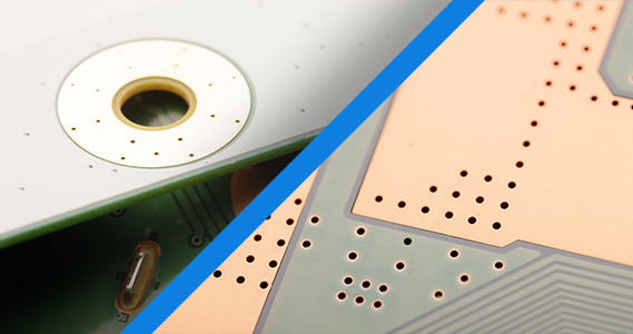
What Is the Difference Between OSP and ENIG? A Complete PCB Finish Comparison
The surface finish selected for printed circuit board (PCB) fabrication is a critical determinant of manufacturing yield, solder joint reliability, shelf life…
Learn more
Gold Plating Standards
Gold is known for its glitter and glamour, but it also has significant value from an electroplating perspective. Why should…
Learn moreStay in touch
